 Shanghai South Ocean Electron Co.,LTD. |
��
|
���� English |
|
Shanghai South Ocean Electron Co.,LTD. |
| Company | Production | Certificate | Technology | Feed Back |
|
1.Technical glossary |
| 1.Technical glossary 1.1 Basic Terminology for Quartz Crystal Resonators Piezoelectric EffectQuartz, composed of Silicon and Oxygen (Silicon Dioxide), exhibits piezoelectric properties. It generates an electrical potential when a pressure is applied on the surfaces of the quartz crystal. Inversely, when an electrical potential is applied to the surfaces of a quartz crystal, mechanical deformation or vibration is generated. These vibrations occur at a frequency determined by: a) the physical dimension of the piece of quartz crystal; b) the cut of the piece in relation to the crystalline axes of the quartz; c) the operating temperature; d) the oscillator circuit. Equivalent Circuit Parameters
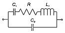
The well-known equivalent circuit used to represent a quartz resonator in the vicinity of the main mode of vibration is shown in the following Figure 1.
It is valid as long as the main mode is isolated from other modes of vibration. Co represents the static capacitance of the electrodes and package, while L1, C1, and R represent the electrical equivalent of the mechanically resonant main mode. The latter are known as motional elements and form the motional arm of the equivalent circuit. Away from the main mode there are many other resonances that can be similarly represented by the parallel addition of other motional arms. When writing a specification for a quartz crystal, the individual parameters of the equivalent circuit should be examined. For all designs, there are limits for each type of crystal design. C0: The shunt capacitance of a crystal is due in part to the thickness of the wafer. This is the measure capacitance while not vibrating. Shunt capacitance ranges from 1 to 7 pF. It is not typical to exceed 7 pF due to compatibility with the oscillator circuit. C1: The motional capacitance of a crystal is determined by the stiffness of the quartz (constant), the area of metalization (electrode size) on the face of the crystal and the thickness and the shape of the wafer. At lower frequencies, the wafer must be shaped (contoured or beveled) to improve the performance of the device. This will lower the C1 of the device. The C1 for fundamental mode crystals can range from approximately 5 fF to 30 fF. As a general rule, if a fundamental design is used on an overtone, the C1 will divide by the square of the overtone (i.e., 3rd overtone will be 1/9 of the fundamental). L1: The motional inductance of the crystal is determined by the mechanical mass of quartz in motion. The lower frequencies (thicker and larger quartz wafers) tend to run at a few Henries, while higher frequencies (thinner and smaller quartz wafers) tend to run at a few milli-Henries. The L1 and C1 are related by Thomson��s formula: L1 = 1/4p2f C1. It is preferable to have the customer specify C1 (if necessary). Then the L1 will follow the above formula. Frequency-Temperature CharacteristicsThe frequency-temperature characteristics are determined by the design of a quartz crystal resonator, the cut angle and the mounting structure. They can be grouped into two types according to the shape of the corresponding curves. One is ternary or third-order, and the other a quadratic or second-order curve. Fig.2 shows an AT-cut characteristic representing a third-order parabola curve. Their inflection point, which depends on the resonator design, is situated between +25��C and +35��C. AT-cut crystal resonators are the most extensively used and are characterized in that they produce small frequency changes in response to temperature changes in the ambient temperature.
Fig.2 AT-cut frequency-temperature characteristics Frequency Tolerance or Calibration AccuracyThe calibration tolerance is the maximum allowable deviation from nominal frequency at a specified temperature (typically 25 degree C). It is normally specified in parts per million (ppm) or percentage of nominal frequency. The overall frequency tolerance is the maximum allowable deviation from nominal frequency due to changes in temperature, time and all other environmental conditions. Frequency StabilityFrequency stability is the maximum allowable deviation from the nominal frequency over a specified temperature range, and is specified in parts per million (ppm) or percentage of nominal frequency. Deviation is usually referenced to the measured frequency at 25 degree C. This parameter depends on the following factors: type of quartz cut, angle of the quartz cut, mode of operation, and mechanical dimensions of the quartz blank. Series Resonance vs. Parallel Load ResonanceA quartz crystal resonator can be used in a circuit to operate in either of the two modes, series or parallel. Series resonant crystal and parallel load resonant crystal are physically the same crystal, but are calibrated to slightly different frequencies. When a crystal is placed into an oscillator circuit, they oscillate together at a tuned frequency. This frequency is dependent upon the crystal design and the amount of load capacitance, if any, that the oscillator circuit presents to the crystal. Load capacitance, specified in pico Farads (pF), is comprised of a combination of the circuit��s discrete load capacitance, stray board capacitance, and capacitance from semiconductor miller effects. When an oscillator circuit presents some amount of load capacitance to a crystal, the crystal is operated at the condition of ��Parallel Load Resonance��, and a value of load capacitance must be specified. Typical values of load capacitance are 18pF, 20pF, 22pF, 30pF and 32pF. The frequency decreases as the value of the load capacitance increases, correlated by the following equation: FL = FS [C1/2(C0 + CL) + 1] Where: FL = Parallel Load
Resonant Frequency (MHz) If the oscillator circuit does not exhibit any capacitive loading, the crystal is operated at the condition of ��Series Resonance��, and no value of load capacitance need to be specified. Crystals operating at series resonance appear resistive in the circuits, and such circuits depend entirely on the crystal unit to provide the phase shift necessary to start and maintain oscillation at the specified frequency. Equivalent Series Resistance (ESR)ESR is the resistive element, measured in Ohms, of a quartz crystal resonator. For crystals designed to operate as series resonance, ESR is the equivalent ohmic resistance of the unit when the motional inductance (L1) and motional capacitance (C1) are of equal ohmic value but are exactly opposite in phase. The net result is that they cancel one another and only a resistance (R) remains in the series leg of the above equivalent circuit (Fig.1). The ESR measurement is made only at the series resonant frequency (FS), not at some predetermined parallel resonant frequency (FL). Crystal resistance measured at some parallel resonant frequency is often called the ��effective�� resistance. Generally, the lower the resistance value of a crystal, the more active it is and less drive is required to activate it. If the ESR is too high, then the crystal may not oscillate. However, lower values than those standard specifications will result in a unit cost increase due to the additional processes required to achieve those ESR values. Drive LevelThe drive level, expressed in microwatts or milliwatts, is the power dissipation level at which the crystal resonator is designed to operate. Maximum power is the most power a crystal resonator can dissipate while still maintaining operation with all electrical parameters guaranteed. Operating the crystal at drive levels that are too high or too low can result in improper performance. For example, if the drive level is too low, the crystal may fail to oscillate or have degraded phase noise performance. On the other hand, if the crystal is driven at too high a level, the results could include frequency shifts (permanent or temporary), crystal activity dips (related to frequency temperature discontinuities), excessive aging or, in extreme case, physical failure of the crystal resonator. In addition, maximum specified ESR of the crystal is affected by and is measured at predetermined drive level. Therefore, it is important to operate the crystal resonator at a suitable drive level.
Fundamental Mode and Overtone Mode
High frequency (MHz range) AT-cut crystals vibrate in the thickness-shear vibration, which can be excited in fundamental or odd overtone modes. The mode of operation of a quartz crystal will determine the frequency of oscillation. For example, a crystal may operate at its fundamental frequency of 10 MHz, or at odd harmonics of approximately 30 MHz (3rd overtone), 50 MHz (5th overtone), and 70MHz (7th overtone). The equivalent circuit of an overtone mode would simply be an additional parallel (R, C1 and L1) branches (no additional C0 branch) equivalent to the fundamental circuit as shown in Fig.1. Overtone crystals are specially processed for plane parallelism and surface finish to enhance its performance at the desired overtone. PullabilityThe pullability of a crystal refers to a crystal operating in the parallel mode and is a measure of the frequency change as a function of load capacitance. The amount of pullability exhibited by a given crystal resonator at a given value of load capacitance is a function of the shunt capacitance C0 and the motional capacitance C1 of the crystal unit, as well as the value of load capacitance. An approximation of the pulling limits for standard crystals can be obtained from the following formula: FL �C FS = FS C1 / 2(C0 + CL) Pullability is important to the circuit designer who needs to obtain several operating frequencies from a crystal unit by changing in values of load capacitance. For example, in certain applications (i.e., VCXO) where variations in the crystals parallel resonant frequency are mandatory, pullability is specified. Spurious Response or Unwanted ModesVibrations at frequencies that are not fundamental or overtone modes of a crystal resonator are referred to as spurious or unwanted modes. All resonating crystal vibrators produce a main mode for each overtone, which is a thickness shear vibration for AT-cut, and also unwanted responses, which are inharmonic thickness shear modes above the resonance frequency. These unwanted response are influenced by many factors including the dimension of the quartz wafer, the surface finish, the size and thickness of the electrode and the mounting technique. In a poorly designed crystal resonator, the ESR of the crystal at the spurious mode can be less than that at the main mode and result in spurious oscillation or frequency jumps in oscillator circuit. Other undesired effects are frequency and resistance dips over temperature caused by unwanted modes. Spurious mode is generally specified in terms of minimum resistance ratio between the spurious mode and the main mode. It is sometimes necessary to specify the suppression of the overtone responses for some oscillator designs. Since all the overtone responses can be excited into vibration, a mode hop from the fundamental to the 3rd overtone can occur. Proper oscillator design may also be needed or desired to reduce circuit modification costs. These modifications can sometimes affect other parameters so it is wise to contact the factory to discuss design options. Aging or Long-Term StabilityLong-term stability or aging of a quartz crystal is a measure of the frequency stability over an extended time period and is usually expressed in terms of parts per million (ppm) per day or year. It applies to the cumulative process which contributes to the deterioration of the crystal unit and which results in a permanent change in operating frequency of the crystal unit. Aging normally follows an exponential progression over time, so that most aging takes place in the first few months after manufacture. This process can be accelerated by operating the crystal at an elevated temperature for an extended, by temperature cycling or by high temperature bake or burn-in. There are many interrelated factors involved in aging. Some of the most common are: internal contamination, crystal surface changes, wire fatigue, small irreversible changes in the crystal lattice, outgassing of the materials, various thermal effects, mounting stresses, and over-driving the crystal. Typical aging figures for metal enclosure crystal units operating in the frequency range of 10 to 20 MHz are 1.0 �C 5.0 ppm / 1st year; while the values for glass enclosure crystals are 0.1 �C 1.0 ppm / 1st yesr. Storage TemperatureThe storage temperature range applies to minimum and maximum temperatures that the devices can be stored or exposed to when in a non-oscillation state. After exposing or storing the device at the minimum or maximum temperatures for a length of time, all of the operating specifications are guaranteed over the specified operating temperature range. �� |
|
1.2 Quartz Crystal Oscillator: Terms and Definitions Nominal frequency: The center or nominal frequency of a crystal oscillator. Package: Crystal oscillators are packaged in various styles from lead through holes to surface mount types. Various sizes and functions are suitable for different applications. Frequency stability: Deviation from the nominal output frequency including the frequency deviation due to manufacturing process, temperature, power source variation and load variation. The most common stabilities are ��25, ��50 and ��100 ppm. Operating temperature range: Temperature range within which output frequency stability and other electrical, environmental characteristics meet the specifications. Military: -55 ��C to +125 ��C; Industrial: -40 ��C to +85 ��C; Commercial: 0 ��C to +70 ��C. Frequency aging: The relative frequency change over a certain period of time. This rate of change of frequency is normally exponential in character. Typically, aging is �� 5 ppm maximum over 1 year Storage temperature: The temperature range within which the unit is safely stored without damaging or changing the performance of the unit. Oscillator output: The output of a hybrid crystal oscillator is a highly stable reference signal and it can form square wave of HCMOS or TTL level, depending on the technology of the active devices used in the circuit. Output logic: The vast majority of systems require a crystal oscillator output that is TTL compatible, CMOS compatible, ECL compatible or some combinations of logic families such as TTL/HCMOS compatible. TTL/HCMOS compatible: The oscillator is designed with ACMOS logic with driving capability of TTL and HCMOS loads while maintaining minimum logic HIGH of the HCMOS. Logic levels: Logic levels may be positive or negative. Positive logic is assumed when logic 1 level is more positive than logic 0 level, while negative logic is assumed when the logic 1 level is more negative than logic 0 level. Output HIGH voltage (VOH): The minimum voltage at output logic 1 state of the oscillator under proper loading. Output LOW voltage (VOL): The maximum voltage at output logic 0 state of the oscillator under proper loading. Fan out (Loads): The measure of the driving capability of an oscillator, expressed as the number of inputs that can be driven by a single output. It can be represented by an equivalent load capacitance specified at pF in CMOS logic or the number of gates in TTL load circuit consisting of diodes, load resistors, and a capacitor. If this value exceeds the maximum rated load of the oscillator, signal degradation can occur. Startup time: The startup time is specified as the time that an oscillator take to reach its specified RF output amplitude. The startup time is determined by the closed loop time constant and the loading condition of its circuit. Rise & Fall time (tr & tf): The rise time tr of an oscillator is defined as the transition time of the output waveform from low stage (logic ��0��) to high stage (logic ��1��). The fall time tf of an oscillator is defined as the transition time of the output waveform from high stage (logic ��1��) to low stage (logic ��0��). The transition time is measured at the specified level such as between 90% and 10% of the falling edge of the switching waveform for HCMOS device. Fast rise & fall time requirements can steer a user to using ECL, even for frequencies typically satisfied by HCMOS/TTL. Increasing the load will increase the rise and fall times of the device. Symmetry or Duty cycle: The measure of output waveform uniformity or the shape of the waveform, which is made up of logic ��1�� and logic ��0�� cycle times. It is defined as the ratio of the time periods of the logic 1 level (TH) to the time periods of one complete cycle (T), measured at 1.4 volts for TTL logic and 50% of the peak-to-peak voltage for CMOS and ECL logic. Sym = TH/T x 100%. Tri-state enable: By applying a command input signal to the oscillators, the output of the clock oscillators is turned off or disabled. When this feature is activated, the oscillators assume a high impedance state. This feature allows the oscillator to be isolated from the circuit upon application of a command signal. Input current and supply voltage: Input current is the amount of current drain by an oscillator in its operating condition. Different logic oscillators require different input current. Supply voltage is the voltage necessary to operate the oscillator. It is typically 5 V or 3.3 V. Phase Noise: Phase noise is a small fraction of undesirable frequency near the output frequency, and is usually expressed as the single side band (SSB) power density in a 1 Hz bandwidth at a specified offset frequency from the carrier. It is measure in dBc/Hz. Jitter: Measure of the modulation in phase or frequency of the oscillator output. Stand by function: A function built in the IC that temporary turns off the oscillator to save power. Logic ��0�� will enable stand by mode. The disable current at stand by mode varies from few microamperes to tens of microamperes (0.005 mA typical). Because oscillation is halted, there is a maximum of 10 ms (same amount as the start-up time) before output stabilizes. Harmonic distortion: The non-linear distortion due to un-wanted harmonic spectrum component related with target signal frequency. Each harmonic component is the ratio of electric power against desired signal output electric power and expressed in terms of dBc. Harmonic distortion specification is important especially in Sine output when a clean and less distorted signal is required. �� |
|
1.3 Voltage Controlled Crystal Oscillators: Terms and Definitions A VCXO is a quartz crystal oscillator that includes a varactor diode and associated circuitry allowing the frequency to be changed by application of a voltage across that diode. By varying the control voltage, the capacitance of the varactor changes accordingly, thus forces the output frequency changed. This can be accomplished in a simple logic clock or sine wave crystal oscillator, or a TCXO (resulting in a TC/VCXO-temperature compensated voltage controlled crystal oscillator), or an oven controlled type (resulting in an OC/VCXO-oven controlled voltage crystal oscillator). In addition to those terms that define the fixed frequency crystal oscillators, there are several characteristics peculiar to VCXOs. Control voltage (VC): An external voltage applied to the input of the VCXO. By changing the voltage, the frequency varies accordingly. Typical VC is 0V to 5V; 0.5V to 4.5V; -0.5V to �C4.5V. Deviation or Frequency pullability: The minimum change in the output frequency with respect to the change in control voltage. Unit is measured in ppm. Standard pullability is ��50 ppm minimum, ��100 ppm minimum. Slope polarity or Transfer function: This denotes the direction of frequency changes with respect to the control voltage. A positive transfer function denotes an increase in frequency for an increasing positive control voltage. Conversely, if the frequency decreases with a more positive (or less negative) control voltage, the transfer function is negative. Linearity: The deviation from the best straight-line slope of the frequency vs. control voltage curve. If the specification for an oscillator requires a linearity of ��10% and the actual deviation is 10 kHz total as an example, the curve of output frequency vs control voltage input could vary as much as ��1 kHz (10 kHz ��10%) from the Best Straight Line. On the other hand, if the maximum deviation from the Best Straight Line is 20 ppm and the total deviation is 200 ppm, the linearity is �� 20 ppm/200 ppm = �� 10%, which is the linearity value for a typical VCXO. Input impedance: A measure of isolation between the input port of the VCXO network and the voltage control source. Typical input impedance is > 50 Ohms @ 10 KHz. Center frequency or nominal frequency: User specified frequency at center control voltage. Standard control voltage for center frequency is 2.5V for 5V applications (with control voltage range 2.5V �� 2.0V) and 1.65V for 3.3V applications (with control voltage range 1.65V �� 1.5V). |
��
|
1.Technical glossary |
|
|